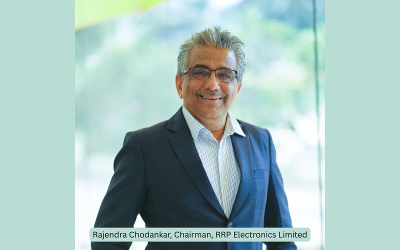
“Our intent is to develop this site in phases, bringing together packaging, advanced wafer-level, packaging, and potential fabrication capabilities over time, along with necessary approvals. This development aligns with the India Semiconductor Mission and the Atmanirbhar Bharat vision.” Rajendra Chodankar, Chairman, RRP Electronics Limited
RRP Electronics Limited, the first company to establish an Outsourced Semiconductor Assembly and Test (OSAT) facility in Maharashtra, has announced the allocation of Industrial Plot No. A-1, measuring approximately 101 acres (about 410,000 square metres), located in Khalapur Phase-3 and Expansion Industrial Area. The land parcel has been earmarked for the development of a large-scale integrated semiconductor manufacturing and advanced packaging campus.
The proposed development is intended to accommodate multiple OSAT (Outsourced Semiconductor Assembly and Test) production lines, advanced wafer-level packaging (WLP) facilities, and potential semiconductor fabrication (fab) units, supported by requisite approvals. The site provides the scale necessary to support phased development aligned with RRP Electronics’ long-term manufacturing roadmap.
Rajendra Chodankar, Chairman, RRP Electronics Limited, said, “The allocation of this ~101-acre land parcel at Khalapur is a foundational step in RRP Electronics’ journey to build a large-scale, integrated semiconductor manufacturing campus in Maharashtra. Our intent is to develop this site in phases, bringing together packaging, advanced wafer-level, packaging, and potential fabrication capabilities over time, along with necessary approvals. This development aligns with the India Semiconductor Mission and the Atmanirbhar Bharat vision. It enables more of the semiconductor value chain to be anchored within the country, strengthening India’s position as a self-reliant and trusted manufacturing hub for global customers.”
The development vision for the Khalapur campus includes co-locating packaging, advanced wafer-level packaging, and potential fabrication capabilities within a single industrial site, enabling operational coordination and future capacity expansion. The planned campus is expected to support manufacturing and research activities serving sectors such as automotive, industrial electronics, telecommunications, and consumer applications, in line with India’s strategic push to deepen domestic semiconductor capabilities.